| Sign In | Join Free | My uabig.com |
|
| Sign In | Join Free | My uabig.com |
|
| Categories | Sapphire Wafer |
|---|---|
| Brand Name: | ZMSH |
| Place of Origin: | SHANGHAI,CHINA |
| MOQ: | 10 |
| Payment Terms: | T/T |
| Delivery Time: | 2-4 WEEKS |
| Material: | Single Crystal Sapphire (Al₂O₃) |
| Purity: | ≥ 99.99% |
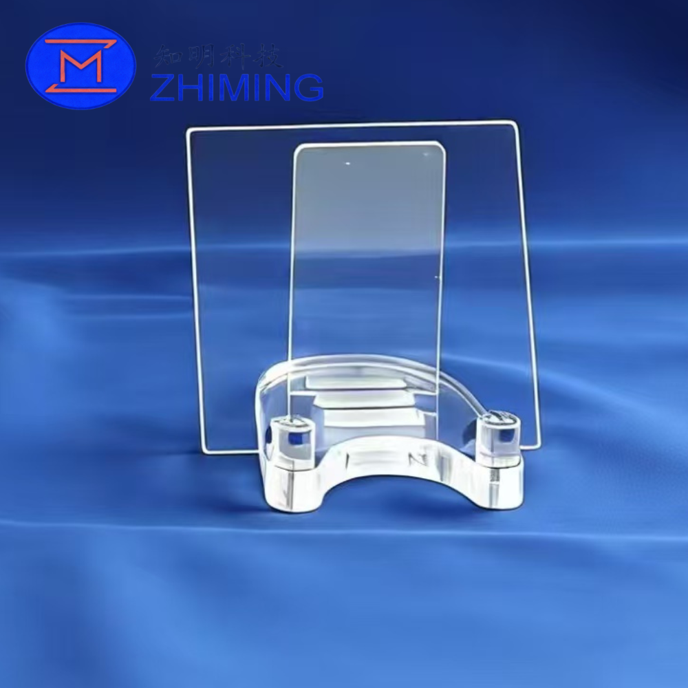
| Shape: | Square |
| Dimensions: | 310 × 310 mm |
| Thickness: | 1.0 mm |
| Thickness Tolerance: | ± 0.02 mm |
| Total Thickness Variation (TTV): | < 10 μm |
| Crystal Orientation: | C-Plane (0001) (others on request) |
| Company Info. |
| SHANGHAI FAMOUS TRADE CO.,LTD |
| Verified Supplier |
| View Contact Details |
| Product List |
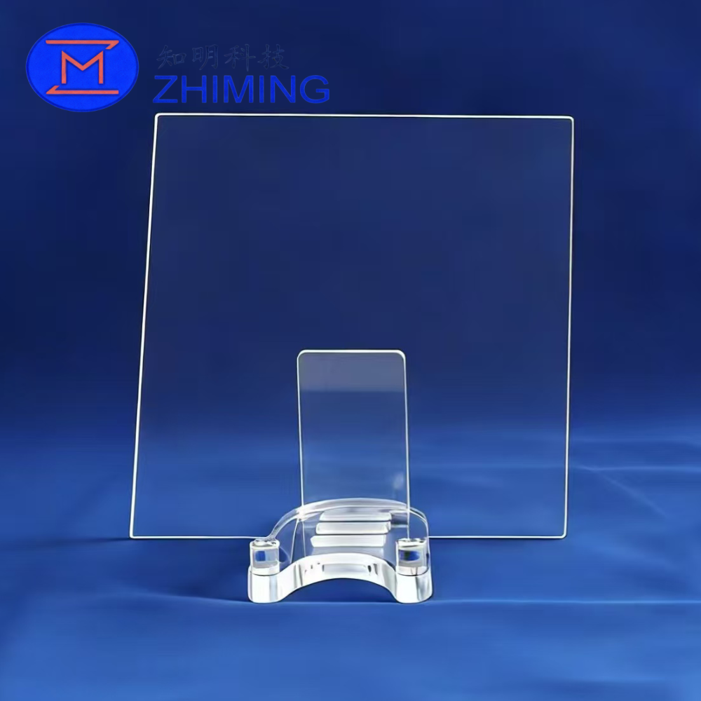
The 310 × 310 × 1 mm Ultra-Large Square Sapphire Substrate represents the upper limit of current synthetic sapphire crystal growth and large-area precision machining technology. Manufactured from 99.99% high-purity single-crystal aluminum oxide (Al₂O₃), this sapphire plate delivers exceptional flatness, thermal stability, chemical resistance, and mechanical strength across an expansive surface area.
Unlike standard round sapphire wafers designed for direct semiconductor production, this product is primarily engineered as a carrier substrate, base plate, or large-area sapphire panel. It is widely used in GaN epitaxial processing, high-temperature semiconductor environments, advanced optical systems, and aerospace applications where dimensional stability and durability are critical.
Semiconductor wafer carrier plates
GaN-on-Sapphire epitaxy (MOCVD)
High-temperature process handling
Large-area optical windows and viewports
Aerospace and vacuum observation windows
Laser system base plates
Precision bonding substrates
Custom industrial and research sapphire platforms
| Parameter | Specification |
|---|---|
| Material | Single Crystal Sapphire (Al₂O₃) |
| Purity | ≥ 99.99% |
| Shape | Square |
| Dimensions | 310 × 310 mm |
| Thickness | 1.0 mm |
| Thickness Tolerance | ± 0.02 mm |
| Total Thickness Variation (TTV) | < 10 μm |
| Crystal Orientation | C-Plane (0001) (others on request) |
| Surface Finish | Double-Side Polished (DSP) |
| Surface Roughness | Ra < 0.2 nm |
| Flatness | λ/10 @ 633 nm |
| Edge Condition | Chamfered or Rounded Corners |
| Optical Quality | Optical Grade |
| Hardness | Mohs 9 |
| Density | 3.98 g/cm³ |
| Thermal Conductivity | ~35 W/m·K @ 25 °C |
| Maximum Operating Temperature | > 1600 °C |
| Chemical Resistance | Excellent (acid & alkali resistant) |
Maintains excellent flatness and thickness uniformity at the 310 mm scale, enabling reliable performance in large-area applications.
With a Mohs hardness of 9, the sapphire surface resists scratching and wear during handling and high-load processing.
Designed to withstand repeated high-temperature cycles commonly encountered in MOCVD and other epitaxial growth processes.
Double-side polishing achieves sub-nanometer surface roughness, making the plate ideal for optical windows and high-strength bonding applications.
Offers significantly higher durability than fused quartz or glass in corrosive and harsh process environments.
Large-scale sapphire boule growth
Precision slicing and stress-relief processing
Double-side polishing (DSP)
Full-surface interferometric flatness inspection
100% visual and dimensional inspection prior to shipment
Q1: Is this product a standard sapphire wafer?
No. This product is classified as an ultra-large sapphire substrate
or carrier plate, not a standard semiconductor wafer. It is
designed for support, optical, or structural applications.
Q2: Can you manufacture sizes larger than 310 mm?
Our current capability for square sapphire substrates ranges from
250 mm to 310 mm per side, depending on orientation and thickness.
Q3: Is it suitable for GaN epitaxial growth?
Yes. This sapphire substrate is widely used as a carrier plate for
GaN-on-Sapphire epitaxial processes, especially in high-throughput
MOCVD systems.
Q4: How is flatness guaranteed on such a large surface?
We use large-format double-side polishing equipment and verify each
plate with laser interferometry to ensure λ/10 flatness at 633 nm.
Q5: How is the substrate packaged for shipping?
Each plate is packed in a custom shock-absorbing, high-cleanliness
vacuum package designed to prevent damage during international
transportation.

|
